Date: 19/02/2024
Keysight's Chiplet PHY Designer to accelerate UCIe chiplet interconnect verification
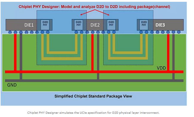
Keysight announced Chiplet PHY Designer to simulate and verify chiplet based die-to-die (D2D) interconnects in a heterogeneous and 3D semiconductor designs. This tool checks your 3D Heterogenous SoC chip designs meeting Universal Chiplet Interconnect Express (UCIe) standard.
Key Features:
Support for UCIe Standard: The Chiplet PHY Designer seamlessly integrates with the UCIe physical layer standard. It automates the parsing of signals, follows standard naming conventions, and establishes automated connections between multiple dies through package interconnects. Additionally, it facilitates standard-driven simulation setup, including speed grade configuration, and offers intuitive measurement setup via specialized probe components.
Voltage Transfer Function (VTF) Measurement: This feature accurately computes the VTF to ensure compliance with UCIe specifications. It analyzes system bit error rate (BER) down to 1e-27 or 1e-32 levels and measures essential parameters such as eye diagram height, eye width, skew, mask margin, and BER contour.
Forwarded Clocking Analysis: The Chiplet PHY Designer enables precise analysis of forwarded clocking to capture asynchronous clocking behavior effectively. This capability enhances the tool's ability to address intricate design considerations and optimize chiplet performance.
Adrien Auge, Senior Staff Applications Engineer, Alphawave Semi, said: The ability to validate Alphawave Semis chiplet solutions is crucial for enabling a future of heterogenous chip design, as it ensures seamless operation and interoperability for 2.5D/3D solutions available to our customers. Chiplet PHY Designer simplifies the electrical simulation process for large die-die electrical connectivity, such as UCIe. It provides engineers and designers a quick and easy path to extract electrical compliance of their solutions against the latest revision of the specification. Furthermore, by complying with the latest IBIS modeling specification for electrical I/O, physical integrators can delve deeper into the chiplet electrical validation process, leveraging our detailed models to obtain pre-silicon performance predictions.
Niels Faché, Vice President and General Manager, Keysight EDA, said: "Our high-speed digital simulation team capitalized on its understanding of the shift left challenges presented by SerDes PHYS. They have applied these learnings to the chiplet domain to extend success of our standards-based simulation strategy to UCIe. Interconnect modeling is critical to system design and performance. Chiplet PHY Designer accelerates validation of chiplet subsystems, from one D2D PHY through interconnect channels to another D2D PHY, much earlier in the design cycle. It enables 3D IC designers to solve critical interconnect performance problems improving predictive virtual prototyping to speed time-to-market."
Tweet Follow @ecewire